- 您现在的位置:买卖IC网 > Sheet目录510 > SI4463-915-DK (Silicon Laboratories Inc)KIT DEV WIRELESS SI4463 915MHZ
�� �
�
�Si4464/63/61/60�
�3.� Enable� PLL.�
�4.� Calibrate� VCO/PLL.�
�5.� Wait� until� PLL� settles� to� required� transmit� frequency� (controlled� by� an� internal� timer).�
�6.� Activate� power� amplifier� and� wait� until� power� ramping� is� completed� (controlled� by� an� internal� timer).�
�7.� Transmit� packet.�
�Steps� in� this� sequence� may� be� eliminated� depending� on� which� state� the� chip� is� configured� to� prior� to� commanding�
�to� TX.� By� default,� the� VCO� and� PLL� are� calibrated� every� time� the� PLL� is� enabled.� When� the� START_TX� API�
�command� is� utilized� the� next� state� may� be� defined� to� ensure� optimal� timing� and� turnaround.�
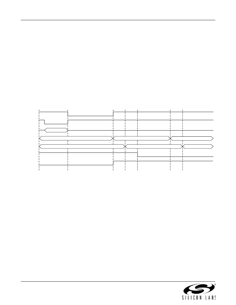
�Figure� 8� shows� an� example� of� the� commands� and� timing� for� the� START_TX� command.� CTS� will� go� high� as� soon�
�as� the� sequencer� puts� the� part� into� TX� state.� As� the� sequencer� is� stepping� through� the� events� listed� above,� CTS�
�will� be� low� and� no� new� commands� or� property� changes� are� allowed.� If� the� Fast� Response� (FRR)� or� nIRQ� is� used� to�
�monitor� the� current� state� there� will� be� slight� delay� caused� by� the� internal� hardware� from� when� the� event� actually�
�occurs� to� when� the� transition� occurs� on� the� FRR� or� nIRQ.� The� time� from� entering� TX� state� to� when� the� FRR� will�
�update� is� 5� μs� and� the� time� to� when� the� nIRQ� will� transition� is� 13� μs.� If� a� GPIO� is� programmed� for� TX� state� or� used�
�as� control� for� a� transmit/receive� switch� (TR� switch)� there� is� no� delay.�
�CTS�
�NSEL�
�SDI�
�START_TX�
�Current� State�
�FRR�
�YYY� State�
�YYY� State�
�Tx� State�
�Tx� State�
�TXCOMPLETE_STATE�
�TXCOMPLETE_STATE�
�nIRQ�
�GPIOx� –� TX� state�
�Figure� 8.� Start_TX� Commands� and� Timing�
�3.3.8.� RX� State�
�The� RX� state� may� be� entered� from� any� of� the� other� states� by� using� the� “Start� RX”� or� “Change� State”� API� command.�
�A� built-in� sequencer� takes� care� of� all� the� actions� required� to� transition� between� states.� The� following� sequence� of�
�events� will� occur� automatically� to� get� the� chip� into� RX� mode� when� going� from� standby� to� RX� state:�
�1.� Enable� the� digital� LDO� and� the� analog� LDOs.�
�2.� Start� up� crystal� oscillator� and� wait� until� ready� (controlled� by� an� internal� timer).�
�3.� Enable� PLL.�
�4.� Calibrate� VCO�
�5.� Wait� until� PLL� settles� to� required� receive� frequency� (controlled� by� an� internal� timer).�
�6.� Enable� receiver� circuits:� LNA,� mixers,� and� ADC.�
�7.� Enable� receive� mode� in� the� digital� modem.�
�Depending� on� the� configuration� of� the� radio,� all� or� some� of� the� following� functions� will� be� performed� automatically�
�by� the� digital� modem:� AGC,� AFC� (optional),� update� status� registers,� bit� synchronization,� packet� handling� (optional)�
�including� sync� word,� header� check,� and� CRC.� Similar� to� the� TX� state,� the� next� state� after� RX� may� be� defined� in� the�
�“Start� RX”� API� command.� The� START_RX� commands� and� timing� will� be� equivalent� to� the� timing� shown� in� Figure� 8.�
�22�
�Rev� 1.2�
�发布紧急采购,3分钟左右您将得到回复。
相关PDF资料
SI4465ADY-T1-GE3
MOSFET P-CH 8V 13.7A 8SOIC
SI4466DY-T1-GE3
MOSFET N-CH 20V 9.5A 8-SOIC
SI4470EY-T1-GE3
MOSFET N-CH D-S 60V 8-SOIC
SI4472DY-T1-GE3
MOSFET N-CH D-S 150V 8-SOIC
SI4477DY-T1-GE3
MOSFET P-CH D-S 20V 8-SOIC
SI4483EDY-T1-GE3
MOSFET P-CH D-S 30V 8-SOIC
SI4484EY-T1-GE3
MOSFET N-CH 100V 8-SOIC
SI4488DY-T1-GE3
MOSFET N-CH 150V 8-SOIC
相关代理商/技术参数
SI4463-915-PDK
制造商:Silicon Laboratories Inc 功能描述:KIT DEV WIRELESS SI4463 915MHZ
Si4463-B0B-FM
功能描述:射频收发器 TRX ROM 63 EZRadioPRO
RoHS:否 制造商:Atmel 频率范围:2322 MHz to 2527 MHz 最大数据速率:2000 Kbps 调制格式:OQPSK 输出功率:4 dBm 类型: 工作电源电压:1.8 V to 3.6 V 最大工作温度:+ 85 C 接口类型:SPI 封装 / 箱体:QFN-32 封装:Tray
Si4463-B0B-FMR
功能描述:射频收发器 TRX ROM 63 EZRadioPRO RoHS:否 制造商:Atmel 频率范围:2322 MHz to 2527 MHz 最大数据速率:2000 Kbps 调制格式:OQPSK 输出功率:4 dBm 类型: 工作电源电压:1.8 V to 3.6 V 最大工作温度:+ 85 C 接口类型:SPI 封装 / 箱体:QFN-32 封装:Tray
SI4463B1BFM
制造商:Silicon Laboratories Inc 功能描述:
Si4463-B1B-FM
功能描述:射频收发器 TRX RoHS:否 制造商:Atmel 频率范围:2322 MHz to 2527 MHz 最大数据速率:2000 Kbps 调制格式:OQPSK 输出功率:4 dBm 类型: 工作电源电压:1.8 V to 3.6 V 最大工作温度:+ 85 C 接口类型:SPI 封装 / 箱体:QFN-32 封装:Tray
Si4463-B1B-FMR
功能描述:射频收发器 TRX RoHS:否 制造商:Atmel 频率范围:2322 MHz to 2527 MHz 最大数据速率:2000 Kbps 调制格式:OQPSK 输出功率:4 dBm 类型: 工作电源电压:1.8 V to 3.6 V 最大工作温度:+ 85 C 接口类型:SPI 封装 / 箱体:QFN-32 封装:Tray
SI4463BDY
制造商:VISHAY 制造商全称:Vishay Siliconix 功能描述:P-Channel 2.5-V (G-S) MOSFET
SI4463BDY-E3
制造商:VISHAY 制造商全称:Vishay Siliconix 功能描述:P-Channel 2.5-V (G-S) MOSFET